ADVANCED MATERIALS
·
2013
·Vol. 25
·期 40
·5750-5755
·
IF 14.829
Jizhong Song,Sergei A. Kulinich,Jian Yan,Zhigang Li,Jianping He,Caixia Kan,Haibo Zeng
Graphical Highly epitaxial ZnO nanowire-on-nanoplate structures as efficient and transferable electron field emitters are reported here. Well-faceted ZnO nanoplates can be used as efficient substrates for the epitaxial growth of nanowires with a sharp and high-quality interface, which significantly improves its field emitter performance. Because of its scalable preparation, high performance and facile transfer, the novel material is of high potential for applications in various optoelectronic devices.
研究领域:
材料科学
·
纳米技术
✓ 已验证
产品关联
DOI
PubMed
高影响因子
Materials
·
2024
·Vol. 17
·期 11
·2758
·
IF 3.1
Guang Xian,Tongxin Zheng,Yaqiu Tao,Zhigang Pan
LaFeO3thin films were successfully epitaxially grown on single-crystalline SrTiO3substrates by the one-step hydrothermal method at a temperature of 320 °C in a 10 mol/L KOH aqueous solution using La(NO3)3and Fe(NO3)3as the raw materials. The growth of the films was consistent with the island growth mode. Scanning electronic microscopy, elemental mapping, and atomic force microscopy demonstrate that the LaFeO3thin films cover the SrTiO3substrate thoroughly. The film subjected to hydrothermal treatment for 4 h exhibits a relatively smooth surface, with an average surface roughness of 10.1 nm. X-ray diffraction in conventional Bragg–Brentano mode shows that the LaFeO3thin films show the same out-of-plane orientation as that of the substrate (i.e., (001)LaFeO3||(001)SrTiO3). The in-plane orientation of the films was analyzed by φ-scanning, revealing that the orientational relationship is [001]LaFeO3||[001]SrTiO3. The ω-rocking curve indicates that the prepared LaFeO3films are of high quality with no significant mosaic defects.
研究领域:
材料科学
·
物理化学
✓ 已验证
产品关联
DOI
PubMed
高影响因子
ACS Applied Optical Materials
·
2024
·
IF 0
Min Yang,Xi Wang,Nan Li,Jiatian Cheng,Chengzhi Xue,Ziwei Xu,Depeng Chu,Xiaojie Zhang,Yucheng Liu,Zhou Yang,Shengzhong Frank Liu
Due to their exceptional responses to X-ray exposure, lead halide perovskites are recognized as ideal candidates for high-spatial-resolution X-ray detectors. However, an effective method to deposit a large-area, submillimeter-thick, dense perovskite film for X-ray detection has been lacking. In this study, a strategy that combines saturated-solution-induced epitaxial growth with a large-area blade-coating process has been developed to produce large-size, submillimeter-thick CH3NH3PbBr3 perovskite films. The successive deposition of a saturated precursor film does not dissolve the underlying perovskite film. Instead, it promotes epitaxial crystal growth by controlling the crystal growth rate over the nucleation rate. The obtained films exhibit a columnar grain structure with fewer pinholes and negligible residual lattice strain. As a result, under an X-ray source with a working voltage of 40 kV, the obtained thick CH3NH3PbBr3 film achieves X-ray sensitivity of up to 1938 μC Gyair–1 cm–2 under −3 V bias, a reduced dark current drift of 1.78 × 10⁻⁴ nA s–1 V–1, and a detection limit of 47 nGyair s–1 under a −2 V bias; all the above are among the best performances reported for the CH3NH3PbBr3-based X-ray detectors. Using the point-to-point current scanning method, a clear X-ray image could be obtained. This study presents an effective approach for producing thick, dense, and crack-free perovskite films directly on substrates for future X-ray detection applications.
研究领域:
材料科学
·
核医学成像
✓ 已验证
DOI
NATURE MATERIALS
·
2022
·Vol. 21
·期 9
·1042-1049
·
IF 47.656
Zhu Zhaohua,Zhu Chao,Yang Lei,Chen Qian,Zhang Linghai,Dai Jie,Cao Jiacheng,Zeng Shaoyu,Wang Zeyi,Wang Zhiwei,Zhang Wei,Bao Jusheng,Yang Lijuan,Yang Yang,Chen Bo,Yin Chunyang,Chen Hong,Cao Yang,Gu Hao,Yan Jiaxu,Wang Nana,Xing Guichuan,Li Hai,Wang Xiaoyong,Li Shaozhou,Liu Zheng,Zhang Hua,Wang Lin,Huang Xiao,Huang Wei
Formation of epitaxial heterostructures via post-growth self-assembly is important in the design and preparation of functional hybrid systems combining unique properties of the constituents. This is particularly attractive for the construction of metal halide perovskite heterostructures, since their conventional solution synthesis usually leads to non-uniformity in composition, crystal phase and dimensionality. Herein, we demonstrate that a series of two-dimensional and three-dimensional perovskites of different composition and crystal phase can form epitaxial heterostructures through a ligand-assisted welding process at room temperature. Using the CsPbBr 3 /PEA 2 PbBr 4 heterostructure as a demonstration, in addition to the effective charge and energy transfer across the epitaxial interface, localized lattice strain was observed at the interface, which was extended to the top layer of the two-dimensional perovskite, leading to multiple new sub-bandgap emissions at low temperature. Given the versatility of our strategy, unlimited hybrid systems are anticipated, yielding composition-, interface- and/or orientation-dependent properties.
研究领域:
材料科学
·
纳米技术
·
光伏技术
·
半导体物理
✓ 已验证
DOI
PubMed
高影响因子
Journal of Nanophotonics
·
2023
·
IF 1.5
Ziheng Wang,Xueying Chu,Jinhua Li,Dengkui Wang
Detectors with cost-effective, polarization-sensitive, and integrative functionalities are required for next-generation ultraviolet (UV) detection systems. Low-dimensional semiconductor materials have potential for optical device applications, especially polarization detection, because of their excellent polarization characteristics. Therefore, ultralong ZnO microwires, ∼0.5 to 1 cm long, were prepared using the chemical vapor-phase epitaxy method, making it easy to build photoelectric devices. The emission polarization of the ZnO microwires excited by circularly polarized light was ∼0.60, indicating a high-anisotropy optical property. Their UV-polarization spectrum and photoelectric detection were determined. When the ZnO microwire was excited by linearly polarized UV light, the intensity of photoluminescence (PL) changed periodically with the polarization direction of the UV light. The PL polarization of the ZnO microwire for linear UV detection was ∼0.12. For a ZnO microwires photoelectric device, the photocurrent anisotropy ratio reached 1.28 when the polarization angle of the incident UV light changed. These results suggest that the obtained ultralong ZnO microwires have the potential for application in future UV-polarization detection systems.
研究领域:
材料科学
·
光学工程
·
半导体器件
✓ 已验证
DOI
高影响因子
JOURNAL OF MATERIALS CHEMISTRY
·
2012
·Vol. 22
·期 21
·10665-10671
·
IF 5.968
Anmin Nie,Jiabin Liu,Qianqian Li,Yingchun Cheng,Cezhou Dong,Wu Zhou,Peng Wang,Qingxiao Wang,Yang Yang,Yihan Zhu,Yuewu Zeng,Hongtao Wang
Taking TiO2/SnO2 core–shell nanowires (NWs) as a model system, we systematically investigate the structure and the morphological evolution of this heterostructure synthesized by atomic layer deposition/epitaxy (ALD/ALE). All characterizations, by X-ray diffraction, high-resolution transmission electron microscopy, selected area electron diffraction and Raman spectra, reveal that single crystalline rutile TiO2 shells can be epitaxially grown on SnO2 NWs with an atomically sharp interface at low temperature (250 °C). The growth behavior of the TiO2 shells highly depends on the surface orientations and the geometrical shape of the core SnO2 NW cross-section. Atomically smooth surfaces are found for growth on the {110} surface. Rough surfaces develop on {100} surfaces due to (100) − (1 × 3) reconstruction, by introducing steps in the [010] direction as a continuation of {110} facets. Lattice mismatch induces superlattice structures in the TiO2 shell and misfit dislocations along the interface. Conformal epitaxial growth has been observed for SnO2 NW cores with an octagonal cross-section ({100} and {110} surfaces). However, for a rectangular core ({10} and {010} surfaces), the shell also derives an octagonal shape from the epitaxial growth, which was explained by a proposed model based on ALD kinetics. The surface steps and defects induced by the lattice mismatch likely lead to improved photoluminescence (PL) performance for the yellow emission. Compared to the pure SnO2 NWs, the PL spectrum of the core–shell nanostructures exhibits a stronger emission peak, which suggests potential applications in optoelectronics.
研究领域:
材料科学
·
纳米技术
✓ 已验证
产品关联
DOI
高影响因子
Frontiers in Chemistry
·
2020
·
IF 3.693
Pan Yuzhu,Wang Xin,Xu Yubing,Li Yuwei,Elemike Elias Emeka,Shuja Ahmed,Li Qing,Zhang Xiaobing,Chen Jing,Zhao Zhiwei,Lei Wei
Introducing hole/electron transporting and blocking layers is considered to enhance the performance of electronic devices based on organic–inorganic hybrid halide perovskite single crystals (PSCs). In many photodiodes, the hole/electron transporting or blocking materials are spin-coated or thermal-evaporated on PSC to fabricate heterojunctions. However, the heterojunction interfaces due to lattice mismatch between hole/electron, transporting or blocking materials and perovskites easily form traps and cracks, which cause noise and leakage current. Besides, these low-mobility transporting layers increase the difficulty of transporting carriers generated by photons to the electrode; hence, they also increase the response time for photo detection. In the present study, MAPbCl3-MAPbBr2.5Cl0.5 heterojunction interfaces were realized by liquid-phase epitaxy, in which MAPbBr2.5Cl0.5 PSC acts as an active layer and MAPbCl3 PSC acts as a hole blocking layer (HBL). Our PIN photodiodes with epitaxial MAPbCl3 PSC as HBL show better performance in dark current, light responsivity, stability, and response time than the photodiodes with spin-coated organic PCBM as HBL. These results suggest that the heterojunction interface formed between two bulk PSCs with different halide compositions by epitaxy growth is very useful for effectively blocking the injected charges under high external electric field, which could improve the collection of photo-generated carriers and hereby enhance the detection performance of the photodiode. Furthermore, the PIN photodiodes made of PSC with epitaxial HBL show the sensitivities of 7.08 mC Gyair−1 cm−2, 4.04 mC Gyair−1 cm−2, and 2.38 mC Gyair−1 cm−2 for 40-keV, 60-keV, and 80-keV X-ray, respectively.
研究领域:
材料科学
·
电子工程
✓ 已验证
DOI
PubMed
高影响因子
RSC Advances
·
2017
·Vol. 7
·期 31
·19205-19210
·
IF 3.108
Jing Yan,Honghu Yao,Junhao Li,Shiman He,Qili Wu,Xianfeng Yang,Wasim Ullah Khan,Jianxin Shi,Mingmei Wu
To meet the increasing requirement, much effort has been devoted to enhance the emission intensity and tailor the emission color of rare earth phosphors. However, limited contributions have been made to the up-conversion (UC) of nanorods by complete epitaxial growth on each facet to achieve this requirement. In this study, we propose a facile epitaxial growth route to grow anisotropic hexagonal β-NaYF4:Yb3+/Ho3+@β-NaYbF4:Er3+, β-NaYF4:Yb3+/Ho3+@β-NaYF4, and β-NaYbF4:Er3+@β-NaYF4 core/shell nanorods, which were realized by adding hexagonal β-NaYF4:Yb3+/Ho3+ or β-NaYbF4:Er3+ nanorods as a core-nanostructure into a solution containing cubic α-NaYbF4:Er3+ or α-NaYF4 nanoparticles as the shell-precursor. During epitaxial growth-induced phase transformation, the precursor nanoparticles disappeared gradually in the solution and consequently corresponding β-phased shell yielded on each outer facet of each β-phased nanorod core. Eventually, the nanorod core was covered completely with a uniformly grown β-NaYbF4:Er3+ or β-NaYF4 shell. The UC emission of either β-NaYF4:Yb3+/Ho3+ or β-NaYbF4:Er3+ core can be enhanced by the outer shell due to the decrease in the number of surface defects. In addition, tailored UC emissions could be obtained by controlling the shell components and thickness, typically in the core/shell nanorods of β-NaYF4:Yb3+/Ho3+@β-NaYbF4:Er3+. The tunable colors with improved emission in these core/shell nanorods may find wider applications in multicolor labeling and anti-counterfeiting.
研究领域:
材料科学
·
光学
✓ 已验证
产品关联
DOI
高影响因子
ACS Applied Electronic Materials
·
2021
·
IF 3.314
Beilei Yuan,Haoming Wei,Jingwei Li,Yu Zhou,Fan Xu,Jinkai Li,Bingqiang Cao
In this paper, inorganic halide perovskite cesium lead bromide (CsPbBr3) films are epitaxially grown on (100)-oriented SrTiO3 substrates by pulsed laser deposition (PLD). This method has the distinctive advantages to grow high-quality films with a precise composition, designed crystalline orientation, and controlled uniform thickness. By optimizing the substrate temperatures and laser pulse numbers, (100)-CsPbBr3 films with uniform morphology are grown on a SrTiO3 substrate via a cubic-on-cubic epitaxial growth mode, which is proven by XRD investigation. Detailed photophysical spectroscopy study including femtosecond transient absorption spectra and detailed low-temperature photoluminescence spectra indicate that such epitaxial CsPbBr3 films are of very low defects in the bandgap. The temperature-dependent resistivity measurement reveals that the epitaxial CsPbBr3 films show a typical thermally activated carrier behavior with a bandgap value of 2.37 eV, which is very consistent with the optical result and indicates a quasi-intrinsic semiconductor nature of such an epitaxial film. Our results confirm that CsPbBr3 films with high crystal quality and lower defect density can be epitaxially grown with PLD for further superlattices and quantum wells.
研究领域:
材料科学
·
物理化学
✓ 已验证
DOI
高影响因子
JOURNAL OF CHROMATOGRAPHY A
·
2015
·
IF 4.169
Tao Bao,Juan Zhang,Wenpeng Zhang,Zilin Chen
Much attention is being paid to applying metal–organic frameworks (MOFs) as stationary phases in chromatography because of their fascinating properties, such as large surface-to-volume ratios, high levels of porosity, and selective adsorption. HKUST-1 is one of the best-studied face-centered-cubic MOF containing nano-sized channels and side pockets for film growth. However, growth of HKUST-1 framework inside capillary column as stationary phase for capillary electrochromatography is a challenge work. In this work, we carry out the growth of HKUST-1 on the inner wall of capillary by using liquid-phase epitaxy process at room temperature. The fabricated HKUST-1@capillary can be successfully used for the separation of substituted benzene including methylbenzene, ethylbenzene, styrene, chlorobenzene, bromobenzene, o -dichlorobenzene, benzene series, phenolic acids, and benzoic acids derivates. High column efficiency of 1.5 × 10 5 N/m for methylbenzene was achieved. The formation of HKUST-1 grown in the capillary was confirmed and characterized by scanning electron microscopy images, Fourier transform infrared spectra and X-ray diffraction. The column showed long lifetime and excellent stability. The relative standard deviations for intra-day and inter-day repeatability of the HKUST-1@capillary were lower than 7%.
研究领域:
分析化学
·
材料科学
✓ 已验证
DOI
PubMed
高影响因子
CRYSTAL GROWTH & DESIGN
·
2025
·
IF 3.4
Yiran Wu,Jinyang Liu,Yulong Lian,Yuzhen Lian,Hongbing Cai
One-dimensional multisegment nanostructures, with their unique physicochemical properties and broad application potential in optoelectronics, have garnered significant attention. However, current synthesis methods face challenges, including strict catalyst requirements, limited control over segment dimensions, and difficulties in achieving scalable and precise fabrication. These obstacles hinder the exploration of size-dependent physical properties and advanced applications. Here, we present a catalyst-free incommensurate heteroepitaxial growth method to synthesize Sb2Se3 multisegment homostructured nanowires. Using dashed-line-like nanowires synthesized in the first step as templates, our method achieves precise control over the segment number (three to nine) and diameter, forming homostructures with distinct physical properties. The Sb2Se3 nanowires grow along the [001] direction, and their anisotropic characteristics were confirmed by angle-resolved polarization Raman spectroscopy (ARPRS). The Sb2Se3 nanowires were applied in polarization-sensitive photodetectors, demonstrating a high dichroic ratio (∼1.7) and strong anisotropic photocurrent responses. This approach provides a versatile and scalable solution for fabricating multisegment nanostructures with tailored properties, paving the way for the further exploration of size-dependent phenomena and their integration into advanced anisotropic optoelectronic devices.
研究领域:
材料科学
·
纳米技术
·
光学工程
✓ 已验证
产品关联
DOI
高影响因子
ADVANCED MATERIALS
·
2024
·
IF 27.4
Zhenyu Liu,Wei Ju,Yongzheng Fang,Dingyue Sun,Xiaohong Zheng,Jingshan Hou,Ning Dai,Kenan Zhang,Yufeng Shan,Yufeng Liu
The heteroepitaxy of 2D materials with engineered bandgaps are crucial to broaden the spectral response for their integrated optoelectronic devices. However, it is a challenge to achieve the high-oriented epitaxy and integration of multicomponent 2D materials with varying lattice constants on the same substrate due to the limitation of lattice matching. Here, in-plane adaptive heteroepitaxy of a series of high-oriented 2D cesium bismuth halide (Cs 3 Bi 2 X 9, X = I, Br, Cl) single crystals with varying lattice constants from 8.41 to 7.71 Å is achieved on c -plane sapphire with distinct lattice constant of 4.76 Å at a low temperature of 160 °C in an air ambient, benefiting from tolerable interfacial strain by switching compressive stress to tensile stress during a 30° rotation of crystal orientation. First-principles calculation demonstrates that those are all thermodynamically stable phases, deriving from multiple minima of interfacial energy between single crystals and sapphire substrate. The detectivity of Cs 3 Bi 2 I 9 photodetector reaches up to 3.7 × 10 12 Jones, deriving from high single-crystal quality. This work provides a promising experimental strategy and basic theory to boost the heteroepitaxy and integration of 2D single crystals with varying lattice constants on low-cost dielectric substrate, paving the way for their applications in integrated optoelectronics.
研究领域:
材料科学
·
光学
·
半导体物理
✓ 已验证
产品关联
DOI
PubMed
高影响因子



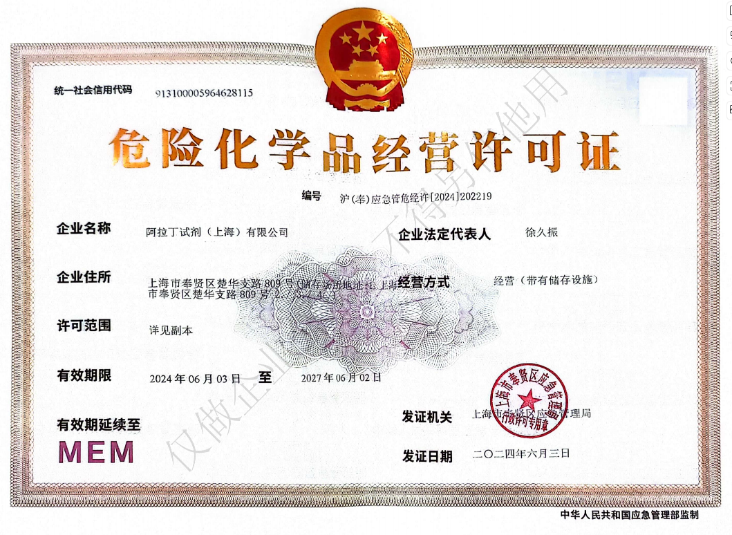 危险品化学品经营许可证(带存储)