CHEMICAL ENGINEERING JOURNAL
·
2025
·
IF 13.2
Yunqi He,Wenfei Wei,Shiping Sun,Yacheng Ma,Ji Li,Zhong Liu
Polyaniline, a notable polymer material, exhibits significant utility in electrical, optical, and thermal due to its unique reversible doping characteristics and physicochemical transformations. The efficiency of nitrogen-containing sites in polyaniline significantly influences its practical performance. This efficiency can be enhanced through molecular engineering by controlling the polymer's structure, degree of polymerization, and morphology. In this study, linear polyaniline with nanotips has been successfully synthesized via regulated voltage during electrochemical polymerization, achieving high-capacity ion extraction and desalination. Low-voltage polymerization eliminated dipolar cations, yielding products containing only quinonoid and benzenoid rings. Furthermore, the lower polymerization degree improved the efficiency of nitrogen-containing sites as electrochemical ion adsorption sites, resulting in a high chloride ion adsorption capacity of 339 mg g −1 and a sodium ion adsorption capacity of 142 mg g −1 . This research advances the development of structurally controllable materials and provides valuable insights into their design, particularly in terms of structural and morphological optimization.
✓ 已验证
产品关联
DOI
高影响因子
Nature Communications
·
2025
·Vol. 16
·期 1
·1-8
·
IF 15.7
Li Yimeng,Xia Linghan,Li Nan,Tang Shilong,Ge Yunsong,Wang Jianyu,Xiao Bing,Cheng Yonghong,Ang Lay Kee,Meng Guodong
Field electron emission is a key mechanism in nanoelectronics with nanogaps, offering advantages such as high electron velocity and fast switching speeds. However, nanoscale field emission, affected by geometric asymmetry including quantum tunneling near to the emitter, and quantum space charge effects, remains largely unexplored in experimental studies. Here, we in situ investigated field emission characteristics of pure tungsten nanotips across vacuum nanogaps. We revealed a widely applicable scaling behavior between field emission characteristics and the ratio of apex radius to gap length ( R/d ), and demonstrated that the effects of quantum tunnelling due to emitter shape are the predominant influence. We further proposed a modified field emission equation, incorporating an empirical formula for the apex shape factor, k MG ( k MG = f ( R / d ) = 1.680 × ( R / d + 0.468) −1.066 ), valid for R / d = 0.04 to 48. These findings provide fundamental insights into the optimization of nanoelectronic device design and the advancement of future technologies.
研究领域:
纳米电子学
·
凝聚态物理
·
表面科学
·
真空微纳电子学
·
场发射器件
✓ 已验证
产品关联
DOI
PubMed
高影响因子
Nature Communications
·
2025
·
IF 15.7
Li Yimeng,Xia Linghan,Li Nan,Wang Jianyu,Tang Shilong,Ge Yunsong,Xiao Bing,Xie Degang,Cheng Yonghong,Shan Zhi-Wei,Djurabekova Flyura,Meng Guodong
Electric-field-induced effects severely impact the long-term stability and reliability of nanoelectronic devices with nanogaps, such as field emission nanodiodes, field-effect nanotransistors and ultrafast switches. However, the damage mechanisms behind nanostructured electrode under high electric fields remain unclear. Here, we investigate deformation behaviors of tungsten nanotips, a typical nanostructured electrode, under an external electric field ( ~ 10 V/nm) using an in situ transmission electron microscopy (TEM), presenting the direct observation of both surface morphological evolution and dislocation dynamics. We find that electron wind effects and nanoscale effects dramatically reduce the atom evaporation threshold to 10-13 V/nm, which is approximately one-fourth to one-fifth of the previously reported values of 40-60 V/nm. Furthermore, we identify a field-induced deformation mechanism where strong electric fields and emission currents generate substantial, size-dependent structural changes closely governed by crystallographic orientation (Wulff shape) without external heating, occurring primarily through field-assisted evaporation rather than conventionally assumed field-induced surface atom diffusion. These findings enhance the understanding of electric-field-induced damage and are crucial for nanoelectronic devices optimization, reliability, and lifetime evaluation.
✓ 已验证
产品关联
DOI
PubMed
高影响因子



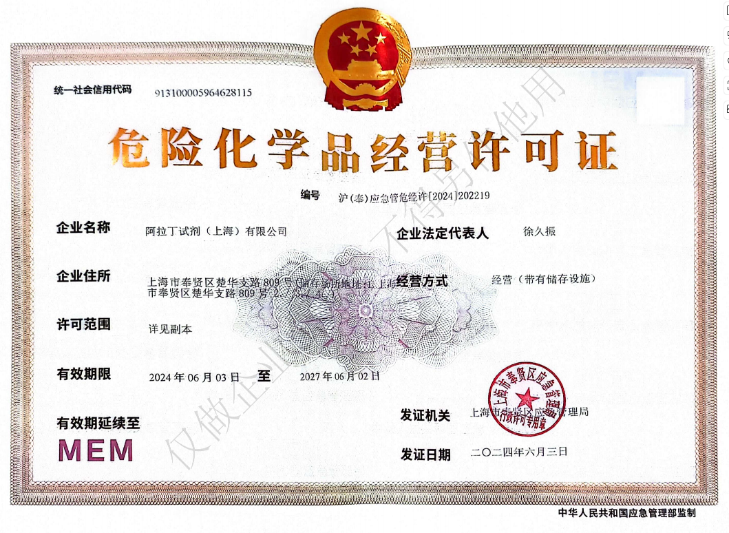 危险品化学品经营许可证(带存储)