Zhenghao He,Zhiqiang Bao,Xiaoyang Guo,Ying Lv,Tienan Wang,Yuejia Ma,Xingyuan Liu
Transparent displays are one of the development directions of future displays, and have great application potential in smart windows, wearable electronic products, virtual reality technology, touch screens and other fields. Perovskite materials have high fluorescence quantum efficiency and high color purity, which make a thin luminous layer achieve high device performance, making us foresee their potential application in the field of transparent displays in the future. However, due to the limitations of the modulation of the luminescent layer and top transparent electrodes, the performance of transparent perovskite light-emitting diodes (TPeLEDs) still has a certain gap compared to the traditional perovskite light-emitting diodes (PeLEDs). In this work, the first blue emitted TPeLEDs were prepared by using quasi two-dimensional perovskite materials and multilayer transparent top electrodes. By designing and optimizing the performance of the luminescent layer and the structure of the top transparent electrode, the transmittance and device efficiency of TPeLEDs were enhanced. The best TPeLED shows a maximum transmittance of nearly 70%, and displays a maximum brightness of 2294 cd m−2 and a maximum external quantum efficiency (EQE) of 11.73%.
Transparent non-emissive displays are ideal for augmented reality (AR) applications due to their ability to modulate ambient light as colored and transparent pixels. Electrochromic (EC) displays with transparent “ON” and “OFF” states can help enable such a display. However, unwanted image diffusion and signal crosstalk due to the imbalance between performance and the preparation process limit their practical application. In this work, we present a transparent and energy-efficient EC display prototype (4.2 inch, 16 × 16 pixels). We minimize the signal crosstalk problem by exploiting the confinement effect between EC pixels using the in situ photolithography of EC materials with the application of a photolithographic pixel definition layer and digital dispensing printing. The prototype has an optical modulation of ∼60%, a full-contrast lifetime tested beyond 20,000 cycles, an ultra-low power consumption (9.5 μW/cm 2 ), and the ability to provide spatiotemporally tunable information for potential AR applications.
Display technology is being revolutionized by cutting-edge transparent displays that can provide visual information on the screen while allowing the surrounding environment to be visible. In this report, a new method is proposed for patterning displays based on perovskite quantum dots (PQDs) on glass surfaces. A glass substrate with a polyvinylidene fluoride (PVDF) constraint layer is patterned using laser-induced plasma etching, and then a PQDs film is spin-coated on the etched sample. The PQDs pattern on the glass substrate is obtained after peeling off the PVDF constraint layer. The thickness of the film is obtained by carrying out simulations. The plasma output from different metal targets is recorded and analyzed to select the most suitable parameters and materials for improvement of the patterning accuracy. The transparent pattern display of PQDs is realized with an accuracy of 10-20 µm and a burial depth of about 1 µm. This method allows PQDs to be encapsulated under the substrate surface, which decreases the susceptibility of environmental impact. Additionally, encapsulation prevents the quantum dots from leaking out and causing environmental pollution. The proposed method has potential in the design of transparent displays and anti-counterfeiting applications.



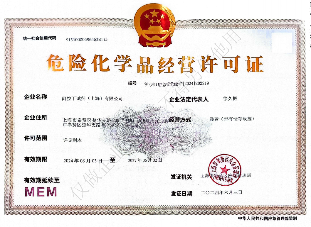 危险品化学品经营许可证(带存储)