SOLAR ENERGY
·
2025
·
IF 6.6
Yan Zhu,Bin Yao,Zhanhui Ding,Yongfeng Li,Liyuan Shi,Chunkai Wang,Ding Ma,Mengge Li,Yue Liu,Ning Ding,Yuting Sun,Xiaofei Sun,Shaung Li
In this work, non-uniform Ag and In co-doped CZTSSe (NoU-Ag x In y , x = Ag/(Ag + Cu) = 0–15 %, y = In/(In + Zn + Sn) = 0–12 %) was prepared by doping Ag at the front surface of CZTSSe and doping In at the back surface of CZTSSe. CZTSSe solar cell with conventional structure but without anti-reflection layer was fabricated by using the NoU-Ag x In y as absorber (Cell-NoU-Ag x In y ). Through optimizing the Ag and In doping concentration, the highest PCE of 11.82 % was achieved in the cell-NoU-Ag x In y with x = 10 % and y = 8 %. It is higher than the highest PCE (9.05 %) of CZTSSe solar cells obtained in this work and the highest PCE (9.45 %) of uniform Ag and In co doped CZTSSe solar cells with similar doping concentrations of Ag and In. Compared to CZTSSe solar cell, the increased PCE of cell-NoU-AgIn is dominantly due to decreased J 0 , followed by increase in J L . The decrease in J 0 is mainly attributed to reduce in number of [2Cu Zn + Sn Zn ] defect clusters and of ZnSe at front interface induced by Ag doping, as well as formation of passivation field at back interface induced by In doping. The increase in J L is mainly due to increase in depletion region width induced by the Ag doping and formation of the passivation field. This study demonstrates that non-uniform Ag and In doped CZTSSe is favorable to increasing PCE of CZTSSe solar cells.
✓ 已验证
产品关联
DOI
高影响因子
Journal of Physical Chemistry C
·
2021
·
IF 4.126
Jiayong Zhang,Ting Wang,Bin Yao,Zhanhui Ding,Yongfeng Li,Chunkai Wang,Jia Liu
High carrier recombination at the Cu2ZnSn (S, Se)4(CZTSSe)/CdS interface is the critical issue that results in the low power conversion efficiency (PCE) of CZTSSe solar cells. To reduce the recombination by optimizing the CZTSSe/CdS interfacial structure, we fabricated a Zn doped CdS (ZnxCd1 – xS) thin film with x of 0–0.32 and a CZTSSe solar cell with the ZnxCd1 – xS as the buffer layer. It is found that Zn substitutes for Cd in the x range of 0–0.26 and that some of the Zn substitutes for Cd and another Zn locates in the interstitial site of the CdS lattice in the x range of 0.26–0.32, which make the lattice mismatch between CZTSSe and ZnxCd1 – xS decrease in x of 0–0.26 and increase in x of 0.26–0.32. The conduction band offset at the CZTSSe/ZnxCd1 – xS interface is demonstrated by XPS to be a positive ″spike″-like type and increases from 0.11 to 0.43 eV as x increases from 0 to 0.32. PCE is increased from 5.00 to 7.73% by optimizing x. The increased PCE is attributed to increased open-circuit voltage (VOC) and filling factor (FF), while the decreased PCE is due to decreased VOC, FF, and JSC. By using quantitative analysis methods, the increased VOC and FF are mainly attributed to the increased shunt resistance (Rsh) and decreased reverse saturation current density (J0), and the decreased short-circuit current density (JSC) is attributed to the increased conduction band offset (CBO). The influence mechanism of Zn doping on Rsh, J0, and CBO is discussed.
研究领域:
材料科学
·
能源科学
✓ 已验证
DOI
高影响因子
JOURNAL OF ELECTRONIC MATERIALS
·
2023
·Vol. 52
·期 8
·5422-5429
·
IF 2.1
Xu Jiaxiong,Wu Xiaoshuai
Chalcogenide Cu 2 ZnSn(S,Se) 4 (CZTSSe) is a promising absorber material for photovoltaic applications. When CZTSSe thin film is deposited on an Mo substrate, a Mo(S,Se) 2 layer easily forms between the CZTSSe and the Mo, which is detrimental to the back contact property of the CZTSSe. This work proposes a useful way to inhibit the formation of Mo(S,Se) 2 by sputtering a CuCrO 2 layer on a Mo-foil substrate before the deposition of the CZTSSe. The effects of CuCrO 2 thickness on the crystalline structures, morphologies, and electrical properties of the fabricated samples were studied. The results showed that the insertion of the CuCrO 2 layer prevented the formation of Mo(S,Se) 2 . As the thickness of the CuCrO 2 increased, the thickness of the Mo(S,Se) 2 layer decreased. The Mo(S,Se) 2 layer was absent from the cross-sectional scanning electron microscopy image when the CuCrO 2 thickness exceeded 85 nm. The back contact resistance of CZTSSe decreased monotonously as the CuCrO 2 layer thickened due to the reduction in the Mo(S,Se) 2 layer thickness. Therefore, by inserting a CuCrO 2 layer to separate the CZTSSe and the Mo-foil, the formation of the Mo(S,Se) 2 layer between them was effectively suppressed, and the back contact properties of the CZTSSe thin film were significantly enhanced.
研究领域:
材料科学
·
光伏技术
·
薄膜太阳能电池
✓ 已验证
DOI
高影响因子
MATERIALS SCIENCE IN SEMICONDUCTOR PROCESSING
·
2021
·
IF 3.927
Qiulian Li,Shizhong Sun,Xinyu Li,Xiang Li,Xiu Liu,Daoyong Zhang,Na Yu,Shurong Wang
Kesterite Cu 2 ZnSn(S,Se) 4 (CZTSSe) is emerging as one of the most promising materials owing to its low-cost, non-toxicity, similar electronic properties with Cu 2 (In,Ga)Se 2 (CIGS). However, the current highest power conversion efficiency (PCE) for CZTSSe device is far below the CIGS because of the high open-circuit voltage (V oc ) deficit and low fill factor (FF). Here, we fabricated CZTSSe thin film from 2-methoxyethanol solutions and investigated the effects of different Sn (Sn 2+ vs Sn 4+ ) oxidation states of precursor solution and selenization temperature on the crystal quality of the CZTSSe thin film and device performances. By characterizations and analyses, we found that incomplete redox reaction caused by the off-stoichiometric component in Sn 2+ precursor solution led to the formation of detrimental secondary phases such as SnSe, Cu 2 Se, and SnSe 2 in the CZTSSe thin film. The existence of volatile SnSe could cause the formation of voids and thus affected the FF and V oc . The reaction from Sn 4+ precursor solution to absorber material avoided the formation of SnSe. Ultimately, the Sn 4+ thin film showed better features in terms of improving crystal quality and reducing V oc deficit that limited the efficiency of kesterite CZTSSe thin film solar cells. Besides, we demonstrated that an appropriate selenization temperature could further reduce the number of secondary phases and improve the surface morphology and crystallinity of the CZTSSe thin film. As a result, we obtained CZTSSe thin film solar cells with 8.27% PCE from the Sn 4+ precursor solution under the selenization temperature of 580 °C.
✓ 已验证
产品关联
DOI
高影响因子
JOURNAL OF ALLOYS AND COMPOUNDS
·
2021
·
IF 5.316
Xiaogong Lv,Chengjun Zhu,Yiming Wang,Lei Wang,Jianming Shi
Kesterite Cu 2 Zn 1- x Cd x Sn(S,Se) 4 (CZCTSSe) alloy thin films were fabricated by the water-based solution approach. The influence of Cd doping on the morphology, phase structure, element valence states, optical, electrical, and device performance were comprehensively examined. Cd was clearly alloyed into the Cu 2 ZnSn(S,Se) 4 (CZTSSe) absorber layer to form the CZCTSSe compound. By controlling the relative Cd content, band gap values ( E g ) of the CZCTSSe thin films were engineered between 1.10 eV and 1.21 eV. In addition, doping with Cd led to the enhancement of grain growth as well as improvement of the conductivity and photoelectric property of the absorber layer. In particular, the CZCTSSe ( x = 0.4) absorber layer exhibited a pure phase, larger grain size, compact and uniform topography, suitable band gap, Cu-poor and (Cd+Zn)-rich composition, higher conductivity and better photoelectric response. Power conversion efficiency (PCE) is improved from 4.37% of the CZCTSSe ( x = 0.0) device to 5.16% of CZCTSSe ( x = 0.4) device, and the increases of short-circuit current ( J sc ) achieved to 8.94 mA/cm 2 . The encouraging results suggest that doping of Cd is an effective way to improve CZTSSe film properties and promote device efficiency.
✓ 已验证
产品关联
DOI
高影响因子
MATERIALS SCIENCE IN SEMICONDUCTOR PROCESSING
·
2024
·
IF 4.2
Wuzhi Zhu,Jiaming Hu,Xiaohui Tan,Fangfang Wu,Xuyuan Chen,Xiuxun Han
Large open-circuit voltage deficit is still the main factor restricting the performance of kesterite Cu 2 ZnSn(S,Se) 4 thin film solar cells. The high concentration of Cu Zn defects and [2Cu Zn + Sn Zn ] defect clusters are believed to be the significant origins of severe band tailing of the kesterite absorber. A promising way to improve the open-circuit voltage and power conversion efficiency of the device is substituting Ag + with a larger ionic radius for Cu + to suppress the defects and construct a front-graded bandgap. However, the Ag doping in kesterite can significantly lower the melting temperature, which results in difficulties in forming an Ag grading distribution across the absorber due to the strong thermal diffusion . Herein, we innovatively introduce a ZnO insert layer in the precursor film, which is expected to slow down the Ag-Cu interdiffusion during the selenization, thereby forming a desired front-graded bandgap. The Ag grading distribution in absorbers is regulated by the thickness of ZnO insert layer. The effects of ZnO insert layer on the phase compositions, morphologies, optical properties , and photovoltaic performance of Ag-doped kesterite absorbers are investigated.
研究领域:
材料科学
·
光伏技术
✓ 已验证
DOI
高影响因子
SOLAR ENERGY MATERIALS AND SOLAR CELLS
·
2023
·
IF 6.9
Jiayong Zhang,Bin Yao,Zhanhui Ding,Yongfeng Li,Ding Ma,Mengge Li,Yuting Sun,Chunkai Wang,Yue Liu,Xiaofei Sun
Although trace silver (Ag) substitution for Cu in Cu 2 ZnSn(S, Se) 4 (CZTSSe) offers benefits in improving open-circuit voltage (V OC ) of CZTSSe solar cells, its further development is still hindered by the fairly low short-circuit current density (J SC ) owing to the increase of bandgap (E g ) of the absorber layer . Herein, a strategy is demonstrated to mitigate the poor J SC arising from the Ag substitution by tuning the Cu 2+ /(Cu + +Cu 2+ ) percentage in the (Cu, Ag) 2 ZnSnS 4 (CAZTS) precursor solution . Depth characterization indicates that the appropriate Cu 2+ /(Cu + +Cu 2+ ) percentage in the CAZTS precursor solution increases the photogenerated charges separation and carrier transport processes for Ag-substituted CZTSSe (CAZTSSe) solar cells. Benefiting from this strategy, the power conversion efficiency (PCE) of 9.57% is achieved when the Cu 2+ /(Cu + +Cu 2+ ) is 50 at.%. The main factor for the improvement of PCE is due to the increase in photogenerated current density (J L ) and decrease in shunt resistance (R sh ). It is demonstrated that the increase in J L results from a widening in the depletion layer width (W d ) of the p-n junction and an increase in carrier lifetime, induced by optimization of the Cu 2+ /(Cu + +Cu 2+ ) percentage. While the decrease in R sh comes from the change of reaction pathways due to the change in Cu 2+ /(Cu + +Cu 2+ ) percentage.
研究领域:
材料科学
·
光伏技术
✓ 已验证
DOI
高影响因子
SOLAR ENERGY
·
2021
·
IF 5.742
Ting Wang,Jiayong Zhang,Bin Yao,Yongfeng Li,Zhanhui Ding,Chunkai Wang,Jia Liu
Five types of Cu 2 ZnSn(S,Se) 4 (CZTSSe) films were fabricated by selenization of Cu 2 ZnSnS 4 (CZTS) precursor films preparing through Cu-Zn-Sn-S precursor solutions with nominal Cu + /(Cu + +Cu 2+ ) ratio of 0, 0.2, 0.4, 0.8 and 1. Five types of CZTSSe solar cells were prepared by using the five types of CZTSSe films as absorbers, respectively. The crystal quality and phase composition of the CZTS and CZTSSe films were characterized by XRD, Raman and SEM, and the photovoltaic performance for the CZTSSe solar cells were measured by J-V and EQE. It is found that the CZTS film consists of kesterite CZTS when the ratio is 0 and of kesterite CZTS together with a small amount of SnS when the ratio is 0.2 to 1. All of the CZTSSe films are comprised of kesterite CZTSSe and a small amount of Zn(S,Se). The crystal quality and lattice constants of the kesterite CZTSSe increase with increasing the ratio, while the amount of Zn(S,Se) decreases with increasing the ratio and almost to zero as the ratio is 1. The power conversion efficiency ( PCE ) of the CZTSSe solar cells increases from 5.47% to 8.43% as the ratio increases from 0 to 1, which is due to improvement in short-circuit current density ( J sc ) and filling factor ( FF ) and decrease in open circuit voltage deficit ( V oc , def ). The influence mechanism of the ratio on the PCE is suggested by analyzing effect of the ratio on electrical parameters of the CZTSSe solar cells.
研究领域:
光伏技术
·
材料科学
·
半导体薄膜
·
太阳能电池技术
✓ 已验证
DOI
高影响因子
ACS Applied Energy Materials
·
2018
·
IF 0
Junjie Fu,Jie Fu,Qingwen Tian,Houlin Wang,Fengming Zhao,Jun Kong,Xiangyun Zhao,Sixin Wu
The Se content in a Cu2ZnSn(S, Se)4 absorber layer has a significant impact on the electronic properties, but it is rather challenging to control the Se/(S + Se) ratio due to a complicated selenization process. Here, a low-toxicity thiol/amine-based solution process was developed to tune the Se content in a Cu2ZnSn(S, Se)4 absorber layer to an optimal value by ingeniously controlling the SeO2 in the precursor solution. We demonstrated that the crystal growth and the band gap of Cu2ZnSn(S, Se)4 thin films are affected by the Se/(S + Se) ratio. By this approach, the open-circuit voltage deficit (Voc,def) of the device was effectively decreased, and the short-circuit density (Jsc) and fill factor (FF) were remarkably improved; thus, the power conversion efficiency of the Cu2ZnSn(S, Se)4 solar cells was successfully increased from 5.6% to 9.7% for the optimal band gap (Eg = 1.13 eV).
✓ 已验证
产品关联
DOI
SEMICONDUCTOR SCIENCE AND TECHNOLOGY
·
2025
·Vol. 40
·期 3
·035006
·
IF 2.1
Xingyu Zhang,Lingling Wang,Yawei Wang,Xiangyang Zhao,Rong Fang,Rui Guo,Yue Zhou,Xintong Zhang,Yichun Liu
Modifying the back contact interface plays a key role in improving the efficiency of Cu2ZnSn(S,Se)4 (CZTSSe) solar cells. Aiming at the phase decomposition and carrier recombination issues in the CZTSSe/Mo back contact interface, an ultra-thin Mg(OH)2 intermediate layer was introduced between the Mo substrate and the CZTSSe absorber layer. The Mg(OH)2 intermediate layer effectively suppressed the interface phase decomposition reactions and inhibited the generation of interface secondary phases. Meanwhile, during the high-temperature selenization process, the Mg2+ doped into CZTSSe at the back contact interface, reducing the defects and band offset at the CZTSSe/Mo interface. The performance of the device was improved, with a significant increase in efficiency compared to the control device. This work highlights the modification effect of Mg(OH)2 for improving back contact and also provides an easy-handling method to achieve high-performance CZTSSe solar cells.
✓ 已验证
产品关联
DOI
高影响因子
ChemSusChem
·
2025
·
IF 6.6
Umar Farooq,Boyang Han,Usman Ali Shah,Fa Yang,Sheng Li,Yanping Song,Ali Hassan,Zhengquan Li,Jin Wang
The efficiency of earth-abundant kesterite Cu2ZnSn(S,Se)4 (CZTSSe) solar cells has been lagging behind the Shockley-Queisser limit primarily due to the presence of deep-level defects. These deep-level defects cause critical issues such as short carrier diffusion length, significant band tailing, and a large open-circuit voltage (VOC) deficit, ultimately leading to low device efficiency. To address these issues, we propose a post-fabrication defect healing strategy by dip-coating the CZTSSe film in dimethylformamide (DMF) solvent. Immersing the absorber layer in DMF (a polar solvent), neutralizes CuSn antisite defects through chemical bonding and facilitates the formation of a dense, smooth CZTSSe film with larger grain size. Deep-level transient spectroscopy revealed a remarkable increase in carrier diffusion length from 93 nm (control device) to 142 nm (champion device), confirming the beneficial effect of solvent-assisted post-treatment on mitigating CuSn antisite defects. The reduction in defect densities led to a decrease in VOC deficit by up to 289 mV, accompanied by an increased champion device efficiency of 11.4%. This work highlights the huge potential of the DMF post-treatment strategy for defect healing in CZTSSe solar cells.
✓ 已验证
产品关联
DOI
PubMed
高影响因子
Journal of Materials Chemistry A
·
2019
·Vol. 7
·期 7
·3135-3142
·
IF 10.733
Xiangyun Zhao,Dongxing Kou,Wenhui Zhou,Zhengji Zhou,Yuena Meng,Qingbo Meng,Zhi Zheng,Sixin Wu
Although low-temperature selenization technology offers several advantages in terms of production costs and beneficial composition profile controlling for Cu2ZnSn(S,Se)4 (CZTSSe) solar cells, excellent performance has not yet been achieved primarily due to the increased number of electronic disorders, smaller grain sizes, and more grain boundaries. In this study, a universal strategy for significantly increasing the power conversion efficiency (PCE) of low-temperature processed CZTSSe solar cells through directly dissolving the fluxing agent antimony into the as-prepared precursor solution is demonstrated. The key feature of this approach is that Sb atoms actually act without entering into the lattice and leave almost no residue within the absorber after taking effect. By appropriately adjusting the antimony incorporation concentration, the grain size, fine-grain layer thickness, local defect chemistry environment, and hole carrier concentration can be simultaneously improved, especially at low temperatures. More importantly, a larger band bending around the grain boundary (GB) is also observed by increasing the potential value from 40 mV to 100 mV after antimony incorporation, which can facilitate the GB-dominated carrier separation process. Due to the antimony-assisted morphology and enhancement in the nanoscale electrical properties, the CZTSSe device could maintain its performance at a lower temperature of 80 °C and directly decrease the selenization temperature down to 470 °C. This systematic study presents a new aspect for overcoming the challenges encountered at low temperatures, and our findings further support the great feasibility for the future application of low-temperature-processed CZTSSe photovoltaic technology to meet the industrial-scale production standards.
研究领域:
材料科学
·
能源技术
✓ 已验证
DOI
高影响因子



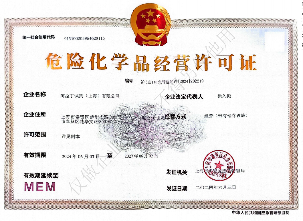 危险品化学品经营许可证(带存储)