ACS Applied Energy Materials
·
2018
·
IF 0
Junjie Fu,Jie Fu,Qingwen Tian,Houlin Wang,Fengming Zhao,Jun Kong,Xiangyun Zhao,Sixin Wu
The Se content in a Cu2ZnSn(S, Se)4 absorber layer has a significant impact on the electronic properties, but it is rather challenging to control the Se/(S + Se) ratio due to a complicated selenization process. Here, a low-toxicity thiol/amine-based solution process was developed to tune the Se content in a Cu2ZnSn(S, Se)4 absorber layer to an optimal value by ingeniously controlling the SeO2 in the precursor solution. We demonstrated that the crystal growth and the band gap of Cu2ZnSn(S, Se)4 thin films are affected by the Se/(S + Se) ratio. By this approach, the open-circuit voltage deficit (Voc,def) of the device was effectively decreased, and the short-circuit density (Jsc) and fill factor (FF) were remarkably improved; thus, the power conversion efficiency of the Cu2ZnSn(S, Se)4 solar cells was successfully increased from 5.6% to 9.7% for the optimal band gap (Eg = 1.13 eV).
✓ 已验证
产品关联
DOI
Journal of Materials Chemistry A
·
2019
·Vol. 7
·期 7
·3135-3142
·
IF 10.733
Xiangyun Zhao,Dongxing Kou,Wenhui Zhou,Zhengji Zhou,Yuena Meng,Qingbo Meng,Zhi Zheng,Sixin Wu
Although low-temperature selenization technology offers several advantages in terms of production costs and beneficial composition profile controlling for Cu2ZnSn(S,Se)4 (CZTSSe) solar cells, excellent performance has not yet been achieved primarily due to the increased number of electronic disorders, smaller grain sizes, and more grain boundaries. In this study, a universal strategy for significantly increasing the power conversion efficiency (PCE) of low-temperature processed CZTSSe solar cells through directly dissolving the fluxing agent antimony into the as-prepared precursor solution is demonstrated. The key feature of this approach is that Sb atoms actually act without entering into the lattice and leave almost no residue within the absorber after taking effect. By appropriately adjusting the antimony incorporation concentration, the grain size, fine-grain layer thickness, local defect chemistry environment, and hole carrier concentration can be simultaneously improved, especially at low temperatures. More importantly, a larger band bending around the grain boundary (GB) is also observed by increasing the potential value from 40 mV to 100 mV after antimony incorporation, which can facilitate the GB-dominated carrier separation process. Due to the antimony-assisted morphology and enhancement in the nanoscale electrical properties, the CZTSSe device could maintain its performance at a lower temperature of 80 °C and directly decrease the selenization temperature down to 470 °C. This systematic study presents a new aspect for overcoming the challenges encountered at low temperatures, and our findings further support the great feasibility for the future application of low-temperature-processed CZTSSe photovoltaic technology to meet the industrial-scale production standards.
研究领域:
材料科学
·
能源技术
✓ 已验证
DOI
高影响因子
Nanomaterials
·
2022
·Vol. 12
·期 22
·3994
·
IF 5.719
Zhanwu Wang,Yingrui Sui,Meiling Ma,Tianyue Wang
Cu2ZnSn(S,Se)4(CZTSSe) films are considered to be promising materials in the advancement of thin-film solar cells. In such films, the amounts of S and Se control the bandgap. Therefore, it is crucial to control the concentration of S/Se to improve efficiency. In this study, Cu2MnxZn1−xSnS4(CMZTS) films were fabricated using the sol-gel method and treated in a Se environment. The films were post-annealed in a Se atmosphere at various temperature ranges from 300 °C to 550 °C at intervals of 200 °C for 15 min to obtain Cu2MnxZn1−xSn(S,Se)4(CMZTSSe). The elemental properties, surface morphology, and electro-optical properties of the CMZTSSe films were investigated in detail. The bandgap of the CMZTSSe films was adjustable in the scope of 1.11–1.22 eV. The structural propeties and phase purity of the CMZTSSe films were analyzed by X-ray diffraction and Raman analysis. High-quality CMZTSSe films with large grains could be acquired by suitably changing the selenization temperature. Under the optimized selenization conditions, the efficiency of the fabricated CMZTSSe device reached 3.08%.Keywords:Cu2ZnSn(S,Se)4film;Mn-doping;solar cells;properties;selenization temperature
✓ 已验证
产品关联
DOI
PubMed
高影响因子
ACS Applied Materials & Interfaces
·
2017
·
IF 7.504
Yanchun Yang,Lijian Huang,Daocheng Pan
In our recent report (ACS Appl. Mater. Interfaces2016, 8, 5308), Li+ ions had been successfully incorporated into the lattice of the selenized Cu2ZnSn(S,Se)4 thin film on a quartz substrate by substituting equivalent Cu+ ions, and Li+ ions was also found to have the little effect on the crystal growth and defect passivation. To further improve the cell performance of Li-doped CZTSSe devices, we conducted the same experiments on the sodium-rich soda-lime glass (SLG) substrate in this study, instead of sodium-free quartz substrate. Surprisingly, only trace amounts of Li (Li/Cu molar ratio ∼1 × 10⁻⁴) were detected in the final CZTSSe thin films; meanwhile, a large amount of sodium was present on the surface and at the grain boundaries of the selenized thin films. A Li/Na exchange mechanism is used to explain this phenomenon. Only on the sodium-free substrate can Li+ ions enter the CZTSSe host lattice, and doping Li+ ions on the SLG substrate are nearly identical to doping Na+ ions.
✓ 已验证
产品关联
DOI
PubMed
高影响因子
Journal of Materials Chemistry A
·
2020
·Vol. 8
·期 42
·22065-22074
·
IF 11.301
Hongling Guo,Gang Wang,Rutao Meng,Yali Sun,Siyu Wang,Shengli Zhang,Jianyu Wu,Li Wu,Guangxing Liang,Hui Li,Yi Zhang
A Li+-doping strategy is a promising route for achieving highly efficient Cu2ZnSn(S,Se)4 (CZTSSe) photovoltaic devices with a large grain absorber layer, high p-type carrier concentration and good band alignment at the Cu2ZnSn(S,Se)4/CdS interface. However, Li+-doped CZTSSe solar cells based on in situ and pre-deposition doping strategies reported thus far generally suffer from massive lithium losses and sodium rejection due to the soda-lime glass substrate. Therefore, simultaneously fulfilling the goals of simple and efficient Li+-doping remains a major technical challenge, which may be addressed, as we demonstrate here, with the development of a Se&LiF co-selenization process. By engineering the band alignment of the Cu2ZnSn(S,Se)4/CdS interface through the Se&LiF co-selenization process, an encouraging efficiency of 11.63% with an open-circuit voltage deficit of 0.583 V has been reached. Furthermore, the crystallinity of the absorber layer and the distribution of copper are improved, and a more copper-poor CZTSSe surface is formed. This novel Li+-doping strategy introduces a new approach towards the goal of high-performance CZTSSe solar cells compatible with a simple manufacturing process and excellent performance.
✓ 已验证
产品关联
DOI
高影响因子
CHEMISTRY OF MATERIALS
·
2014
·
IF 8.535
Qingwen Tian,Gang Wang,Wangen Zhao,Yanyan Chen,Yanchun Yang,Lijian Huang,Daocheng Pan
We developed a versatile and environmentally friendly solution approach for the fabrication of a variety of metal sulfide nanocrystal thin films. Metal oxides, metal hydroxides, metal chlorides, metal acetates, and metal acetylacetonates can be used as the starting materials and dissolved in thioglycolic acid and ethanolamine, forming many types of metal–organic precursor solutions. High quality CdS, SnS, CuInS2, CuSbS2, Cu2ZnSnS4, Cu(In0.7Ga0.3)S2, and luminescent Ag-doped ZnxCd1–xS nanocrystal thin films have been successfully prepared by spin-coating their corresponding metal precursor solutions. Cu2ZnSn(S,Se)4 thin film solar cell with a power conversion efficiency of 6.83% has been realized by this versatile method.
✓ 已验证
产品关联
DOI
高影响因子
Nature Communications
·
2023
·Vol. 14
·期 1
·1-9
·
IF 16.6
Xu Xiao,Zhou Jiazheng,Yin Kang,Wang Jinlin,Lou Licheng,Jiao Menghan,Zhang Bowen,Li Dongmei,Shi Jiangjian,Wu Huijue,Luo Yanhong,Meng Qingbo
Kesterite Cu 2 ZnSn(S, Se) 4 is considered one of the most competitive photovoltaic materials due to its earth-abundant and nontoxic constituent elements, environmental friendliness, and high stability. However, the preparation of high-quality Kesterite absorbers for photovoltaics is still challenging for the uncontrollability and complexity of selenization reactions between metal element precursors and selenium. In this study, we propose a solid-liquid/solid-gas (solid precursor and liquid/vapor Se) synergistic reaction strategy to precisely control the selenization process. By pre-depositing excess liquid selenium, we provide the high chemical potential of selenium to facilitate the direct and rapid formation of the Kesterite phase. The further optimization of selenium condensation and subsequent volatilization enables the efficient removal of organic compounds and thus improves charge transport in the absorber film. As a result, we achieve high-performance Kesterite solar cells with total-area efficiency of 13.6% (certified at 13.44%) and 1.09 cm 2 -area efficiency of 12.0% (certified at 12.1%).
研究领域:
材料科学
·
光伏技术
·
太阳能
·
半导体物理
✓ 已验证
DOI
PubMed
高影响因子
ACS Applied Materials & Interfaces
·
2019
·
IF 8.456
Yanping Song,Bin Yao,Yongfeng Li,Zhanhui Ding,Huanhuan Sun,Zhenzhong Zhang,Ligong Zhang,Haifeng Zhao
Cu2ZnSn(S,Se)4 (CZTSSe) thin-film solar cells have been encountering a bottleneck period since the champion power conversion efficiency (PCE) of 12.7% was achieved by Kim et al. in 2014. One of the critical factors that impede its further development is the relatively low open-circuit voltage (VOC) caused by serious interface carrier recombination. In this regard, back surface field (BSF) employment is a feasible strategy to address the VOC issue of CZTSSe solar cells to some extent. Here, we demonstrated a self-organized BSF introduced by prompting interfacial MoSe2 layer transition from inherent n-type to desirable p-type with Nb doping (p-MoSe2:Nb). The BSF application can significantly reduce the carrier recombination at the back electrode interface (BEI) and lower down the back contact barrier height. The PCE of the corresponding cell was improved from 4.72 to 7.15% because of the enhancement of VOC and fill factor, primarily stemming from the doubling aspects of increased shunt resistance (RSh), decreased series resistance (RS), and alleviative recombination velocity of the BEI induced by the BSF. Our results suggest that introducing a BSF fulfilled with p-MoSe2:Nb is a facile and promising route to improve the performance of CZTSSe thin-film solar cells.
研究领域:
光伏技术
·
薄膜太阳能电池
·
半导体材料
·
材料科学
·
可再生能源
✓ 已验证
DOI
高影响因子



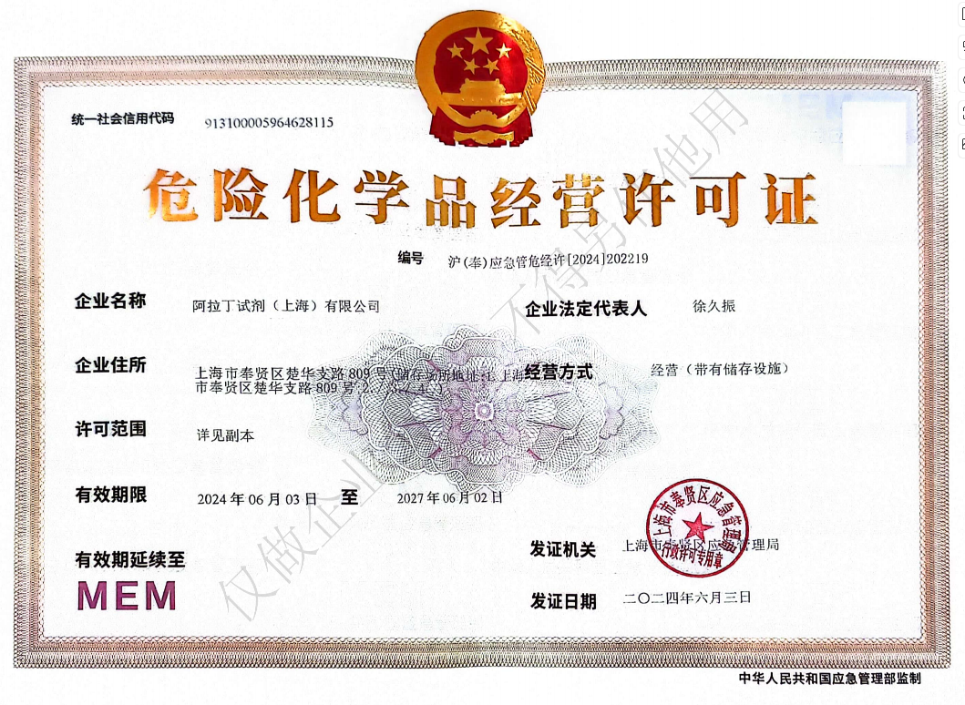 危险品化学品经营许可证(带存储)