In printed circuit board (PCB) fabrication and metal patterning processes, we often need to remove excess copper so that only the required traces and pads remain. The key step that enables this is etching—using a chemical solution to selectively dissolve the unprotected areas of the metal ...
At present, with the rapid development of science and technology, semiconductor materials have become a shining pearl in the field of science and technology, widely penetrating into all aspects of our lives.



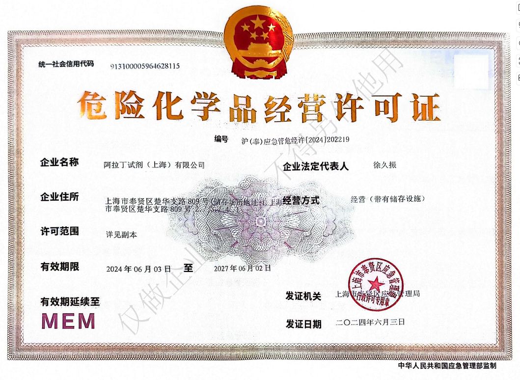 危险品化学品经营许可证(带存储)